VHDL: 8 Bit DipSwitch
A few weeks before I started this project, my friend sent me a video of a lab that he had completed for school. The lab consisted of wiring and programming an Arduino and some seven segment displays to display the decimal number corresponding to the binary number imputed by 8 dip switches. The video he sent me is linked below.
Having just picked up an Altera DE2 development board from Facebook marketplace, I thought that recreating this project would be the perfect way to get an introduction to FPGA programming. Thus, the 8-bit dipswitch project was born.
Getting Started
Before starting this project, I thought that FPGA development was a very interesting subject.
However, I had never done any proper research into the subject, let alone tried to write code for it.
After some preliminary research, I decided that eventually I wanted to learn both VHDL and Verilog at least to a basic degree. I had the opportunity to discuss this with some third-year students currently learning the subject in one of their courses and shortly after decided that I would start with VHDL.
After a quick google search, I found the VHDLWhiz YouTube tutorial series. This was a great series to follow along with and I highly recommend it to anyone trying to learn HDL programming. The series teaches various important skills and tools such as how to create a mux, flipflop, concurrent processes, clocked processes, project test benches, processes and if statements, as well as module instantiation.
FPGA programming is very different to anything I have done before as code runs simultaneously rather than sequentially. Another thing is that since everything within the FPGA is an electrical signal, you cannot leave anything undefined.
Writing the Code
Since VHDL is not chip specific, I started writing the code inside of the ModelSim HDL Simulator. Since this was going to be a simple program, I decided to write all the code within the top module.
As with all the VHDLWhiz tutorials, I started writing the code by declaring the inputs and outputs I would need. Looking at the DE2 Development Board, each of the 8 onboard seven segment displays was a common anode display with six cathode pins going directly to the Cyclone II FPGA chip. To keep the program simple, I decided to use eight dip switches which required three of the seven segment displays.
Below is the top module entity, which instantiates each of the required ports. As you can see, the pins for the displays are all outputs while the switches are marked as inputs.
1
2
3
4
5
6
7
8
9
10
11
12
entity segment is
port(
    -- Inputs
    switches   : in std_logic_vector(7 downto 0);

    -- Outputs
    DispSeg1 : out std_logic_vector(6 downto 0);
    DispSeg2 : out std_logic_vector(6 downto 0);
    DispSeg3 : out std_logic_vector(6 downto 0)

);
end entity;
The next step in writing the code was creating the architecture of the program. I started by creating signals to store the single digit numbers on each display. In hindsight, these did not need to be 8 bits long, but for a simple demonstration program like this it is not worth it to make this change after the fact.
1
2
3
4
5
6
architecture rtl of segment is

-- Numbers for the display
signal Seg1 : unsigned(7 downto 0) := (others => 'X');
signal Seg2 : unsigned(7 downto 0) := (others => 'X');
signal Seg3 : unsigned(7 downto 0) := (others => 'X');
The next thing I did was create a function that turns the single digit numbers into the correct LED illumination for the seven segment displays. The function I created is pictured below:
1
2
3
4
5
6
7
8
9
10
11
12
13
14
15
16
17
18
19
20
pure function f_sevenSegment( num : unsigned(7 downto 0) := (others => 'X') )
    return std_logic_vector is
        variable DispSeg : std_logic_vector(6 downto 0);
begin
    case num is
        when "00000000" => DispSeg := "1000000";
        when "00000001" => DispSeg := "1111001";
        when "00000010" => DispSeg := "0100100";
        when "00000011" => DispSeg := "0110000";
        when "00000100" => DispSeg := "0011001";
        when "00000101" => DispSeg := "0010110";
        when "00000110" => DispSeg := "0000010";
        when "00000111" => DispSeg := "1111000";
        when "00001000" => DispSeg := "0000000";
        when "00001001" => DispSeg := "0011000";
        when others =>
            DispSeg := (others => 'X');
    end case;
    return DispSeg;
end function;
Lastly, I created four unclocked processes. The first process is sensitive to changes in the dipswitches. When any of the dipswitches are changed, the process runs and updates the single digit numbers on each of the seven segment displays.
1
2
3
4
5
6
process(switches, Seg1, Seg2, Seg3) is
begin
    Seg1 <= unsigned(switches)     mod 10;
    Seg2 <= unsigned(switches)/10  mod 10;
    Seg3 <= unsigned(switches)/100 mod 10;
end process;
The other three processes are identical. They all use their respective single digit numbers in their sensitivity lists. They all also serve the same purpose of converting and displaying the number on their respective display.
1
2
3
4
5
6
7
8
9
10
11
12
13
14
process(Seg1) is
begin
    DispSeg1 <= f_sevenSegment( num => Seg1);
end process;

process(Seg2) is
begin
    DispSeg2 <= f_sevenSegment( num => Seg2);
end process;

process(Seg3) is
begin
    DispSeg3 <= f_sevenSegment( num => Seg3);
end process;
Creating the Test Bench
After writing the code, it was necessary to create a test bench to ensure the code was performing as expected. While the code above is synthesizable (able to run on an FPGA), testbench code is specially designed for simulation and is not. Testbench code can usually be easily identified by either having an empty entity structure, or by the sim keyword in the architecture statement.
Creating a test bench is reasonably easy. The first step is to create the signals that will be mapped to the module you are trying to test.
1
2
3
4
5
6
7
8
9
10
11
12
architecture sim of segmentTB is

    -- dip switch "inputs" (simulated)
    signal Switches : std_logic_vector(7 downto 0) := (others => '0');

    -- Segments
    signal Seg1     : std_logic_vector(6 downto 0) := (others => 'X');
    signal Seg2     : std_logic_vector(6 downto 0) := (others => 'X');
    signal Seg3     : std_logic_vector(6 downto 0) := (others => 'X');


begin
The second step is to instantiate the module you are trying to test and map the corresponding signals.
1
2
3
4
5
i_Segment : entity work.segment(rtl) port map (
    switches   => Switches,
    DispSeg1   => Seg1,
    DispSeg2   => Seg2,
    DispSeg3   => Seg3);
Lastly, write some test case code just like you would in any other programming language. For this program, I wrote some code that changes the dipswitches readings every ten nanoseconds.
1
2
3
4
5
6
7
8
9
10
11
12
13
14
15
16
17
18
19
20
21
22
23
24
test : process is
begin
    wait for 10 ns;
    Switches <= "00000001";
    wait for 10 ns;
    Switches <= "00000010";
    wait for 10 ns;
    Switches <= "00000011";
    wait for 10 ns;
    Switches <= "00000100";
    wait for 10 ns;
    Switches <= "00000101";
    wait for 10 ns;
    Switches <= "00000110";
    wait for 10 ns;
    Switches <= "00000111";
    wait for 10 ns;
    Switches <= "00001000";
    wait for 10 ns;
    Switches <= "00010000";
    wait for 10 ns;
    Switches <= "00010100";
    wait;
end process;
Running the Test Bench
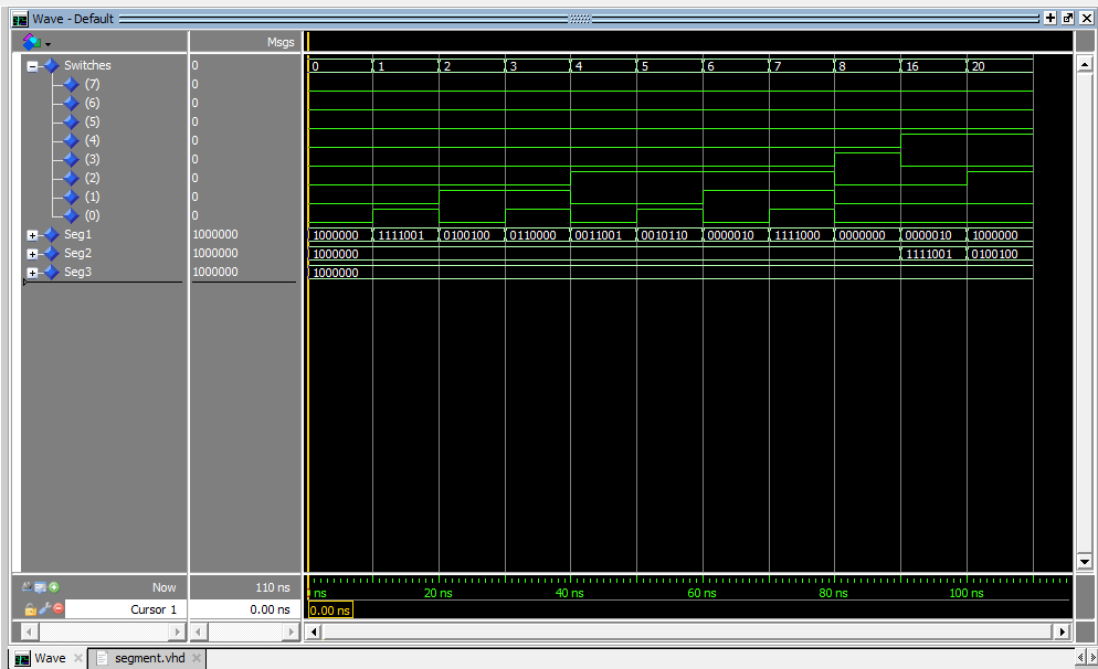
Now that I have created the synthesizable code and its corresponding test bench, its time to run it using a simulation tool. I was recommended to use Altera ModelSim by some peers who were currently learning about the subject in 3rd and 5th year university.
Below is a screenshot of the waveforms generated by ModelSim. Upon checking this with the expected behavior, the program appears to be functioning correctly.
Uploading to the DE2 FPGA
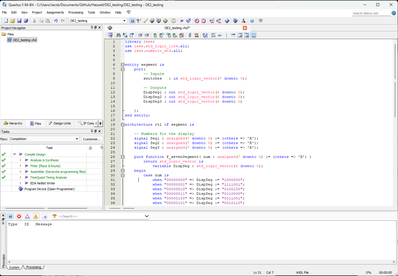
Once I created a project within Quartus II, I copied the main file from my testbench into the project folder and set it as the top-level entity. Luckily everything compiled on the first try and I had minimal issues with Quartus itself.
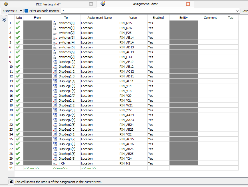
I then set up the pin assignments as follows and recompiled the project.
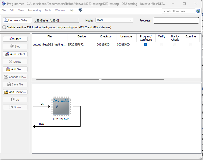
That is not to say it was a complete breeze. Getting the correct drivers for the USB Blaster onboard the DE2 proved to be quite a struggle. Luckily the internet came to the rescue, and I was able to get the board detected within the Quartus II Programming Utility.
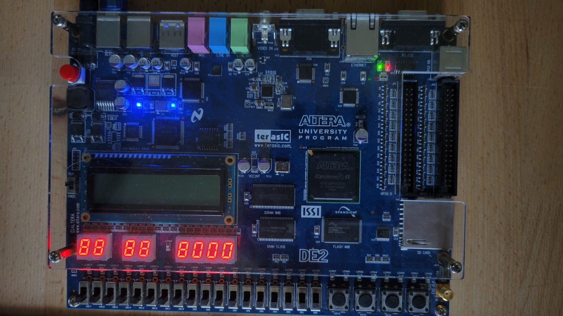
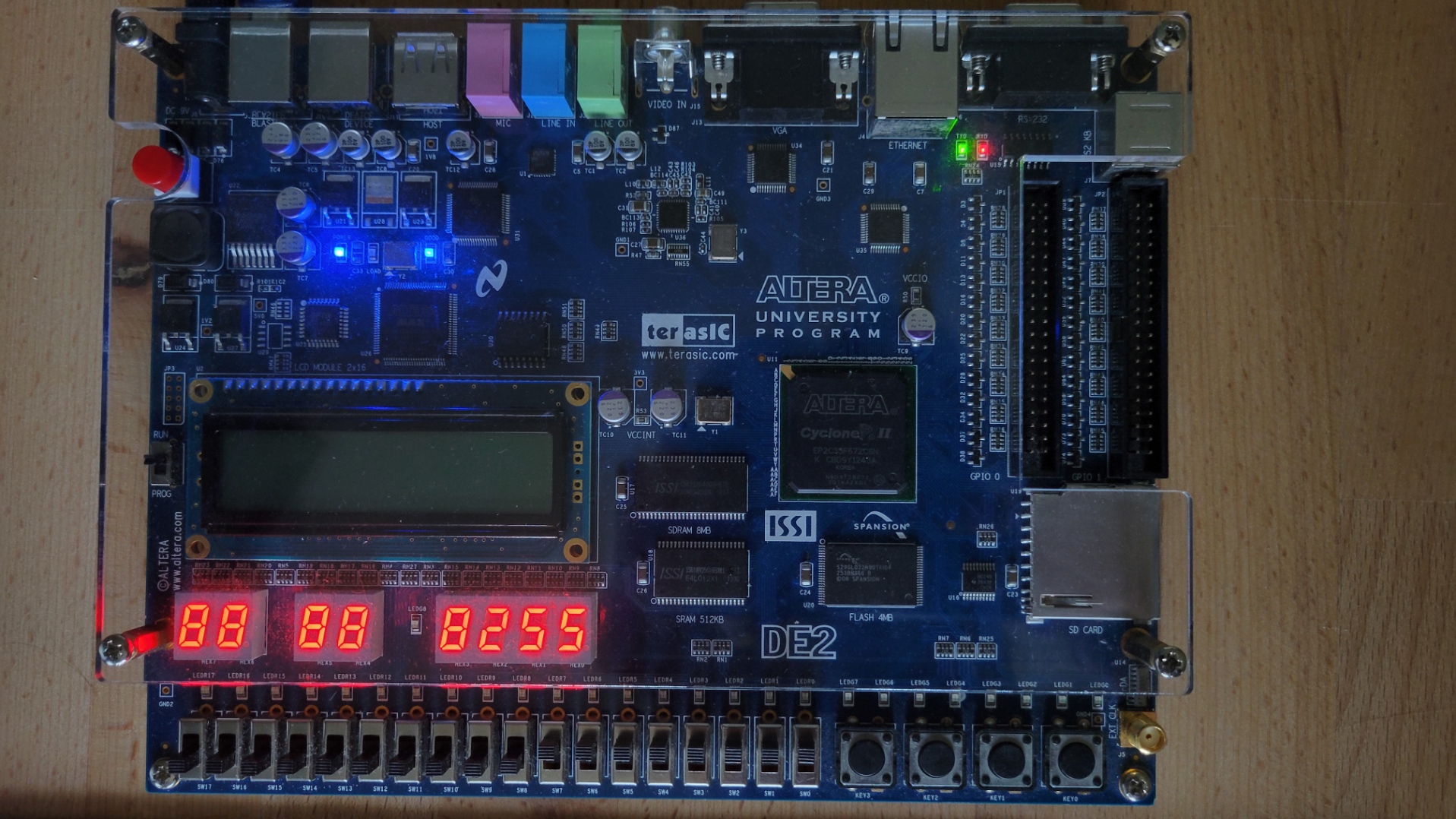
Running the Program
Finally, I got to run and test the code on the Altera DE2 Development board.
Final Remarks
Doing this project has not only been fun, but I have also learned a lot in the process. Hardware Description Languages (HDL) share some similarities with typical programming,but are also very different in a lot of ways. With this project, I was able to gain fundamental skills working not only with Altera Quartus, but also ModelSim. For anyone looking to get into this type of programming, I would not hesitate to read through the ModelSim manual and try to simulate some designs. Learning the ModelSim command line definitely made using the program a little more enjoyable and a lot faster. I hope to continue furthering my knowledge in HDL and FPGA development. Next, I hope to examine building a design with a clocked process.