MiniSRC CPU Design
This report presents the design, implementation, and evaluation of the MiniSRC CPU, a 32-bit RISC-based processor architecture supporting integer arithmetic, including multiplication and division.
Project Specification
The CPU consists of 32 registers and uses an instruction format similar to the NIOS II processor. The registers and their purposes are shown below:
- PC<31..0>: 32-bit Program Counter (PC)
- IR<31..0>: 32-bit Instruction Register (IR)
- R[0..15]<31..0>: 16 32-bit registers, named R[0] through R[15]
- R[0]<31..0>: 1 Constant zero register
- R[1..7]<31..0>: 7 General-Purpose Registers
- R[8]<31..0>: Return Address Register (RA)
- R[9]<31..0>: Stack Pointer (SP)
- R[10..13]<31..0>: Four Argument Registers
- R[14..15]<31..0]: Two Return Value Registers
- RASH<31..0>: (Register ALU Storage Hi) 32-bit Register dedicated to keep the high-order word of a Multiplication product, or the Remainder of a Division operation
- RASL<31..0>: (Register ALU Storage Low) 32-bit Register dedicated to keep the low-order word of a Multiplication product, or the Quotient of a Division operation
Instruction Set Specification
The MiniSRC instruction set consists of five instruction formats. The R and I formats are used for Arithmetic and Logic Unit (ALU) operations, while the J and B instruction formats are used for jumps and branches. The M format is used for special instruction such as halt. Instruction formats are shown below:
1
2
3
4
5
6
7
8
9
10
11
12
13
14
15
16
17
// R Type instruction macro
`define INS_R(code, ra, rb, rc) {code, ra, rb, rc, 15'd0}

// I Type instruction macro
// 19 bit constant C
`define INS_I(code, ra, rb, c) {code, ra, rb, c}

// B Type instruction macro
// 19 bit constant C
// 4 bit constant c2
`define INS_B(code, ra, c2, c) {code, ra, 2'b00, c2, c}

// J Type instruction macro
`define INS_J(code, ra) {code, ra, 23'd0}

// M Type instruction macro
`define INS_M(code) {code, 27'd0}
Processor Design
The original MiniSRC processor follows a bus-based architecture. The following section details the design of a 5-stage pipeline that adheres to the functionality of the MiniSRC instruction set architecture.
5-Stage Datapath
The datapath is a conventional 5-stage pipeline consisting of a register file, ALU, and several intermediate registers and multiplexers. Shown below is the pipeline diagram:

Register File
The register file contains 15 registers marked 0 through 15. The zero register is always zero. Each register can store up to one word (32 bits). The register file has two read ports and one write port. The read ports are multiplexed via an and/or network using two 4 to 16 decoder. The write addressed is decoded via a 4 to 16 demultiplexer used as the register load enable. The functional diagram of the register file is shown below: 
ALU Design
The ALU, or Arithmetic Logic Unit, takes in the three inputs, A and B, along with the control input and produces the high/low arithmetic results. Each input is passed to the functional units within the ALU. Results are multiplexed based on the applied control signals. Additionally, the ALU handles exceptions and edge cases such as integer overflow.
Adder Design
The adder consists of four 8-bit carry look-ahead adders. Ripple carry is used to connect the adders into a single 32 bit adder.
Divisor Design
The divisor is a 32-bit array divider that performs non-restoring division. The divider was constructed using a generate statement for the first 31 stages. The final stage was created separately to implement the final restore.
Multiplier Design
The Multiplier is capable of performing multiplication of 2, 32-bit signed 2’s-complement numbers. The algorithm employs a 2-bit booth encoding to reduce the number of summands from 32 to 16. The summands are then left shifted accordingly and sign extended to align to a width of 64 bits. The 16 summands are then added together using 3 layers of 4-to-2 carry-save adders (https://www.geoffknagge.com/fyp/carrysave.shtml). The final 2 summands output from the final 4-to-2 carry-save adder are added using a carry-propagate adder to produce the final product.
Rollover/Bit Shifting Design
Rollover and bit shifting use the same basic logical design. The two only differ in the bits added to the number. For rollover, the bits are rolled over to the other side of the number. For bit shifting, zeros are placed on the right-hand side while the left-hand side is either sign-extended or is also filled with zeros. The design consists of five stages, with each stage containing a multiplexer that selects between the output from the previous multiplexer, or the manipulated output. This allows for simple, fast manipulation of numbers.
Full Data Path
Below is the full data path diagram:
Control Unit
The control unit handles instruction decoding and issues control signals to the data path. The control unit is split into two fundamental parts: Decode and Issue.
The decode section of the control unit is akin to the decode section in a pipelined processor. It decodes the operation code into several one bit signals that indicate the exact type of the instruction and the format of its operands. The R-type instruction decoding is shown below as an example.
1
2
3
4
5
6
7
8
9
10
11
12
// Assign R-Format Wires
assign OP_ADD = (ID_OpCode == `ISA_ADD);
assign OP_SUB = (ID_OpCode == `ISA_SUB);
assign OP_AND = (ID_OpCode == `ISA_AND);
assign OP_OR  = (ID_OpCode == `ISA_OR);
assign OP_ROR = (ID_OpCode == `ISA_ROR);
assign OP_ROL = (ID_OpCode == `ISA_ROL);
assign OP_SRL = (ID_OpCode == `ISA_SRL);
assign OP_SRA = (ID_OpCode == `ISA_SRA);
assign OP_SLL = (ID_OpCode == `ISA_SLL);
// Opcode Format Wire (Useful for data path MUX Assignments)
assign OPF_R  = (OP_ADD || OP_SUB || OP_AND || OP_OR || OP_ROR || OP_ROL || OP_SRL || OP_SRA || OP_SLL);
The second section of the control unit is instruction issue. Using the decoded signals, the instruction issue assigns the control signals for the datapath multiplexers. In a pipelined CPU, the output of this stage would be sent into the first pipeline register. However, in this non-pipelined version, a five wide ring counter is used to maintain the current processor state.
Control Unit Diagram

Note that the decode module shown above is a simply a decomposition of the Instruction Register (IR) fields. The decode module code is shown below:
1
2
3
4
5
6
7
assign oCode  = iINS[31:27];
assign oRa    = iINS[26:23];
assign oRb    = iINS[22:19];
assign oRc    = iINS[18:15];
assign oImm32 = , iINS[18:0]};
assign oBRD   = , iINS[18:0], 2'b00};
assign oBRC   = iINS[20:19];
Simulations
The following section details the results of several simulations run to verify the workings of the processor.
ALU Simulations
As ALU simulations carry many edge cases, only a subset of cases were tested for this project.
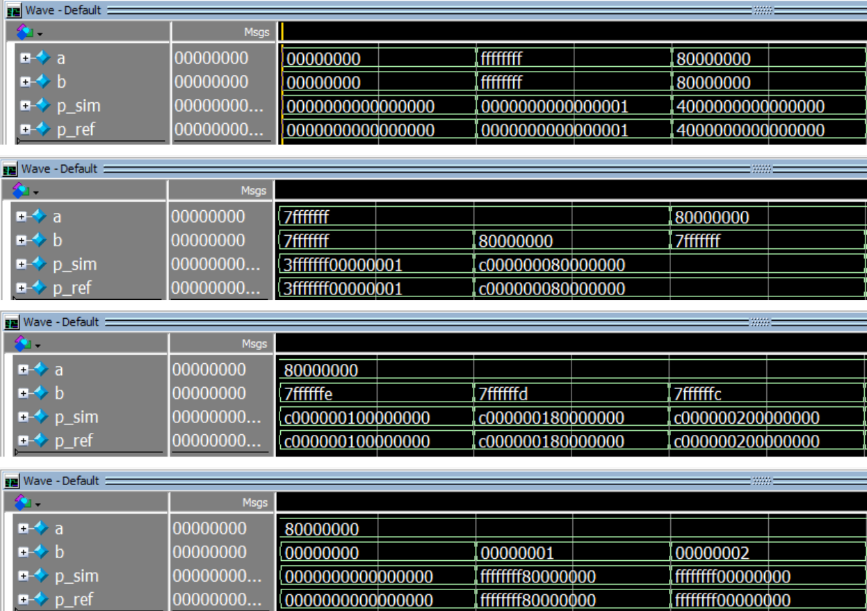
Adder Simulation
The following figure depicts a standalone simulation of the adder. In this simulation, a set of test vectors were applied to the inputs. Note that the ref_sum variable is the sum created using the Verilog + operator. 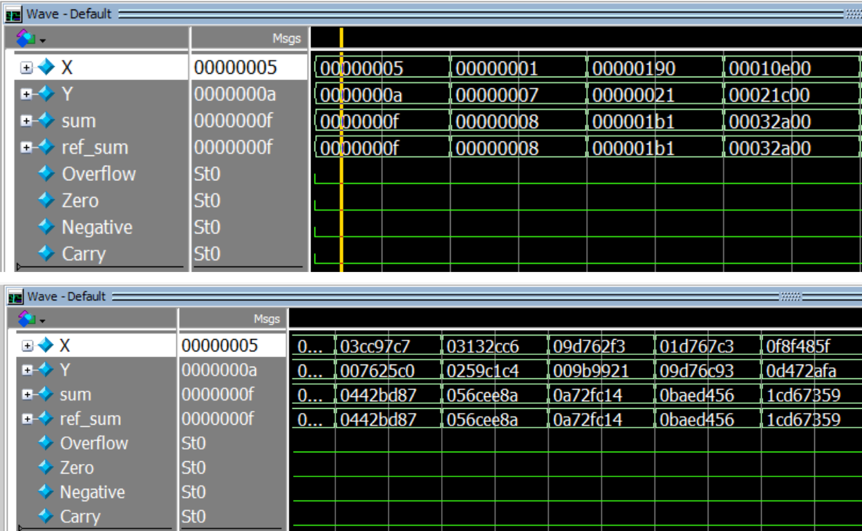
The following simulation tests the adder inside the datapath. In this simulation, the test instruction addi R1, R1, 5 is executed. At the start of the simulation, R1=55. Note that the result written back to the register is 60.
Bit Shift Simulation
The following simulation tests the bit shift module outside the datapath. 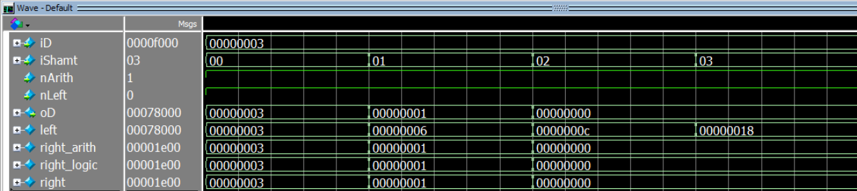
Rollover Simulation
The following simulation tests the rollover module outside the datapath. 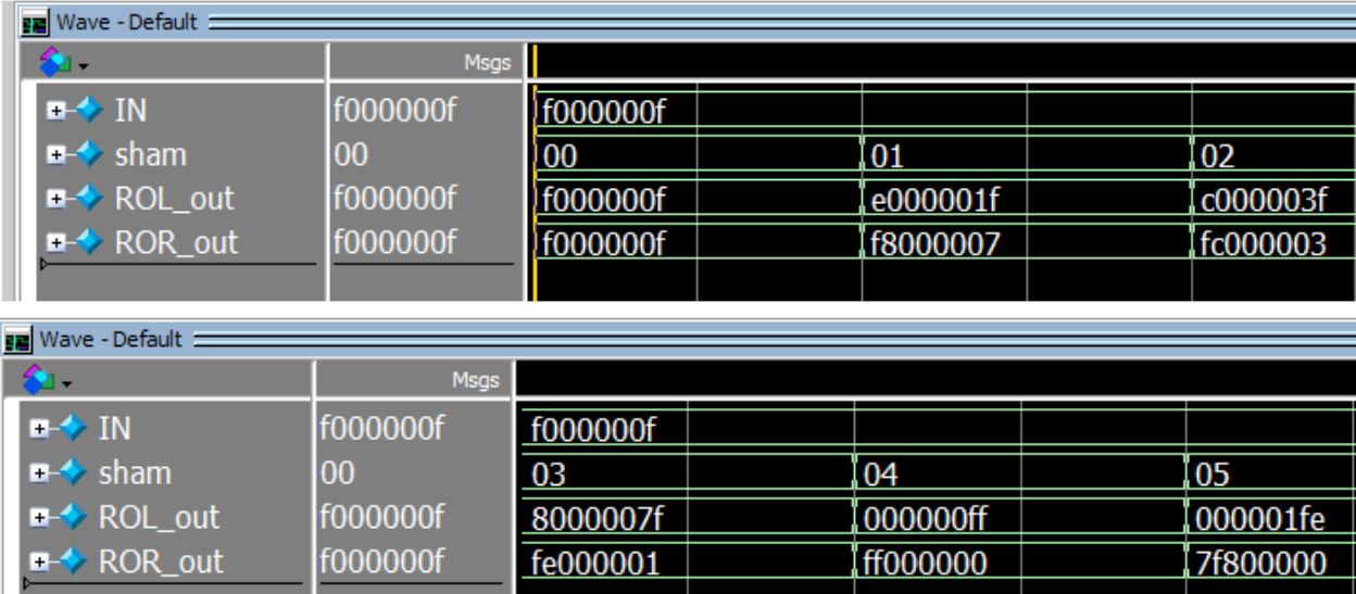
Divisor Simulation
The following simulation tests the divisor module outside the datapath. 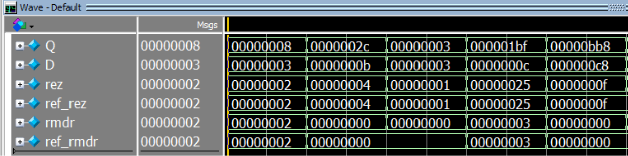
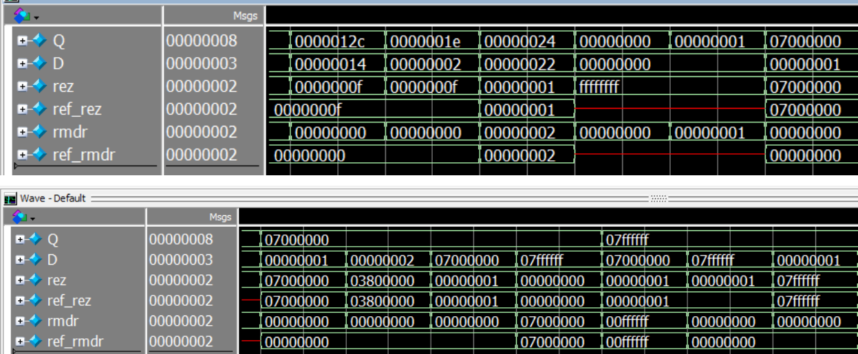
Note that in the divide by zero case, the divisor will return a quotient of zero and a remainder of all ones.
Multiplier Simulation
Load and Store Simulations
Load Simulation
The following simulation tests the instruction lw R1, 0x14(R0). As expected, the processor reads the value from memory in the 4th cycle and writes it back to R1 in the 5th cycle. 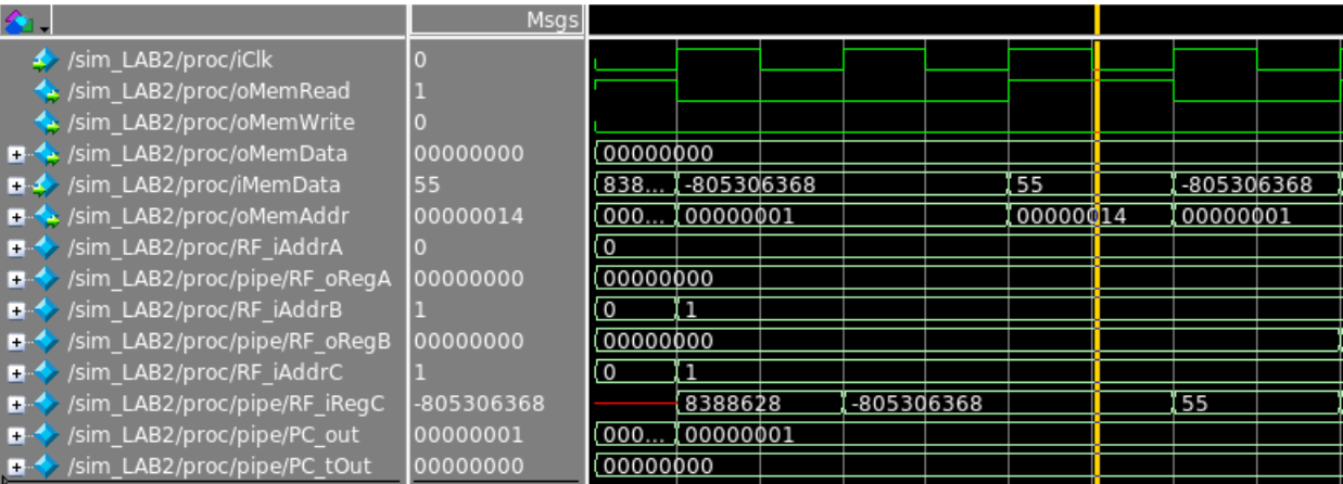
Store Simulation
The following simulation tests the instruction sw R1, 0x2(R0). Note the initial R1 = 55. As expected, the processor writes the value out to memory in the 4th cycle. 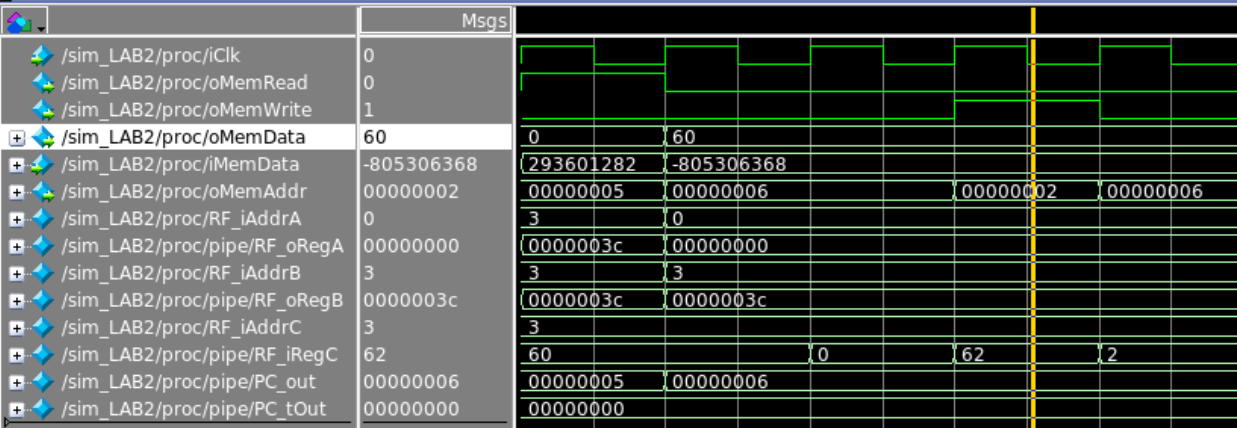
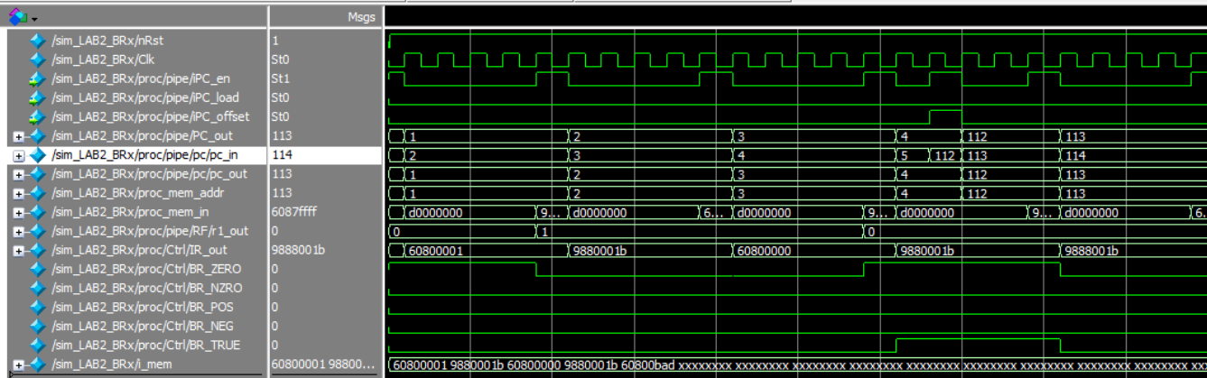
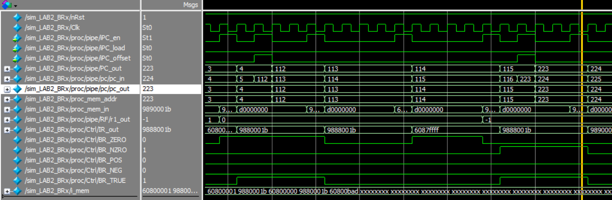
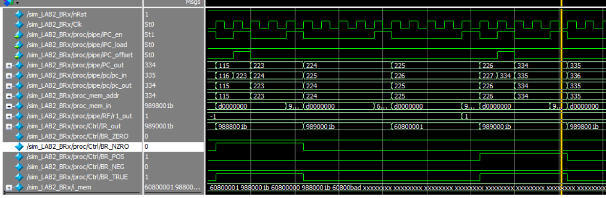
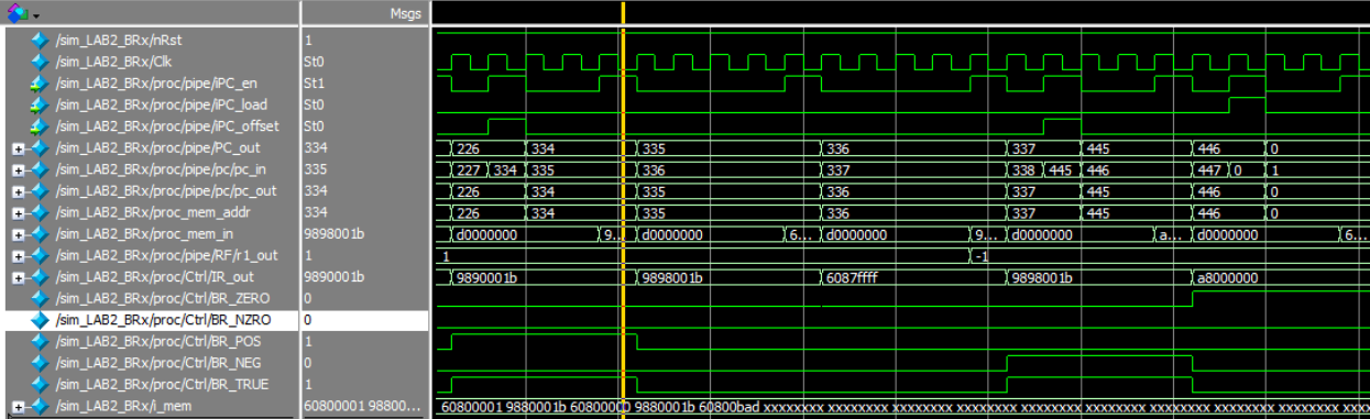
Branch Instruction Simulations
Branch if Zero
Branch if Not Zero
Branch if Positive
Branch if Negative
Processor Code
The full processor code is available on the MiniSRC GitHub. I have placed the top module below:
1
2
3
4
5
6
7
8
9
10
11
12
13
14
15
16
17
18
19
20
21
22
23
24
25
26
27
28
29
30
31
32
33
34
35
36
37
38
39
40
41
42
43
44
45
46
47
48
49
50
51
52
53
54
55
56
57
58
59
60
61
62
63
64
65
66
67
68
69
70
71
72
73
74
75
76
77
78
79
80
81
82
83
84
85
86
87
88
89
90
91
92
93
94
95
96
97
98
99
100
101
102
103
104
105
106
107
108
109
110
111
112
113
114
115
116
117
118
119
120
121
122
123
124
125
126
127
128
129
130
131
132
133
134
135
136
137
138
139
140
141
142
143
144
145
146
147
148
149
150
151
152
153
module Processor(
    iClk, nRst,
    oMemAddr, oMemData,
    iMemData, iMemRdy,
    oMemRead, oMemWrite,
    iPORT, oPORT
);

`include "constants.vh"

input wire iClk, nRst, iMemRdy;
output wire oMemRead, oMemWrite;
input wire [31:0] iMemData;
output wire [31:0] oMemData, oMemAddr;
input wire [31:0] iPORT;
output wire [31:0] oPORT;

// Program Counter Signals
wire PC_nRst, PC_en, PC_tmpEn, PC_load, PC_offset;

// Register File IO
wire RF_iWrite;
wire [3:0] RF_iAddrA, RF_iAddrB, RF_iAddrC;
wire RWB_en;

// ALU IO
wire [3:0]  ALU_iCtrl;
wire ALU_oZero, ALU_oNeg;

// ALU Immediate Registers
wire RA_en, RB_en;
wire RZH_en, RZL_en;
// ALU Storage Registers
wire RAS_en;

// Jump/Branch Signals
wire J_zero, J_nZero, J_pos, J_neg;

// External Port Signals
wire REP_en;
wire [31:0] REP_in;

// Multiplexer Signals
wire MUX_BIS, MUX_RZHS, MUX_WBM, MUX_MAP, MUX_ASS, MUX_WBP, MUX_WBE;

// Control Signals
wire [31:0] CT_imm32;

// Control Unit
Control Ctrl(
    // Clock, reset and ready signals
    // Ready is an active high that allows the next step to continue
    .iClk(iClk),
    .nRst(nRst),
    .iRdy(iMemRdy),
    // Memory Signals/Control
    .iMemData(iMemData),
    .oMemRead(oMemRead),
    .oMemWrite(oMemWrite),
    // Pipe Control
    .oPipe_nRst(pipe_rst),
    // Program Counter Control
    .oPC_nRst(PC_nRst),
    .oPC_en(PC_en),
    .oPC_tmpEn(PC_tmpEn),
    .oPC_load(PC_load),
    .oPC_offset(PC_offset),
    // Register File Control
    .oRF_Write(RF_iWrite),
    .oRF_AddrA(RF_iAddrA),
    .oRF_AddrB(RF_iAddrB),
    .oRF_AddrC(RF_iAddrC),
    .oRWB_en(RWB_en),
    // ALU Control
    .oALU_Ctrl(ALU_iCtrl),
    .oRA_en(RA_en),
    .oRB_en(RB_en),
    .oRZH_en(RZH_en),
    .oRZL_en(RZL_en),
    .oRAS_en(RAS_en),
    // Jump Feedback
    .iJ_zero(J_zero),
    .iJ_nZero(J_nZero),
    .iJ_pos(J_pos),
    .iJ_neg(J_neg),
    // External Port Register Enable
    .oREP_en(REP_en),
    // Multiplexers
    .oMUX_BIS(MUX_BIS),
    .oMUX_RZHS(MUX_RZHS),
    .oMUX_WBM(MUX_WBM),
    .oMUX_MAP(MUX_MAP),
    .oMUX_ASS(MUX_ASS),
    .oMUX_WBP(MUX_WBP),
    .oMUX_WBE(MUX_WBE),
    // Imm32 Output
    .oImm32(CT_imm32)
);

Datapath pipe(
    // Clock and reset signals (reset is active low)
    .iClk(iClk),
    .nRst(pipe_rst),
    // Memory Signals
    .iMemData(iMemData),
    .oMemAddr(oMemAddr),
    .oMemData(oMemData),
    // Port Signals
    .iPORT(iPORT),
    .oPORT(REP_in),
    // Program Counter Control
    .iPC_nRst(PC_nRst),
    .iPC_en(PC_en),
    .iPC_tmpEn(PC_tmpEn),
    .iPC_load(PC_load),
    .iPC_offset(PC_offset),
    // Register File Control
    .iRF_Write(RF_iWrite),
    .iRF_AddrA(RF_iAddrA),
    .iRF_AddrB(RF_iAddrB),
    .iRF_AddrC(RF_iAddrC),
    // Write Back Register Control
    .iRWB_en(RWB_en),
    // ALU Control
    .iALU_Ctrl(ALU_iCtrl),
    .iRA_en(RA_en),
    .iRB_en(RB_en),
    .iRZH_en(RZH_en),
    .iRZL_en(RZL_en),
    .iRAS_en(RAS_en),
    // Jump Feedback
    .oJ_zero(J_zero),
    .oJ_nZero(J_nZero),
    .oJ_pos(J_pos),
    .oJ_neg(J_neg),
    // ALU Results
    .oALU_neg(ALU_oNeg),
    .oALU_zero(ALU_oZero),
    // Multiplexers
    .iMUX_BIS(MUX_BIS), // ALU B Input/Immediate Select
    .iMUX_RZHS(MUX_RZHS), // ALU Result High Select
    .iMUX_WBM(MUX_WBM), // Write back in Memory Select
    .iMUX_MAP(MUX_MAP), // Memory Address out PC Select
    .iMUX_ASS(MUX_ASS), // ALU Storage Select
    .iMUX_WBP(MUX_WBP),
    .iMUX_WBE(MUX_WBE),
    // Imm32 Output
    .iImm32(CT_imm32)
);

REG32 REP(.iClk(iClk), .nRst(nRst), .iEn(REP_en), .iD(REP_in), .oQ(oPORT));

endmodule
Credits
- Jacob Chisholm
- ALU
- Divisor
- Adder
- Bit Manipulation Logic (Shift, Roll, …)
- Data Path
- Register File
- Processor Module
- Control Unit
- Unit Test Benches
- Processor Test Bench Template
- ALU
- Hendrix Gryspeerdt
- ALU
- Multiplier
- Lab Test Benches
- Lab 1
- Lab 3
- Lab 4 (Simulation)
- ALU